


Foreword:
By controlling the on/off state of the high-side and low-side MOSFETs, the capacitor is repeatedly charged and discharged, and the maximum current value during instantaneous discharge is observed. Simulation software is used to study the maximum discharge current value of the capacitor resulting from different forms of large-area copper pours (PADS terminology). The purpose and significance of this circuit is to study and verify the different discharge current values caused solely by differences in PCB layout, under the same MOSFET and capacitor values (ignoring the results caused by minor parameter differences between components). The results calculated by the simulation software provide directions for improvement, and a physical prototype is manufactured for final observation.
This result also clarifies how the noise generated during the operation of digital ICs is transmitted and affects other devices, and how it leads to excessive radiation in electronic products (IEC61000 and GB/T 17626 standards).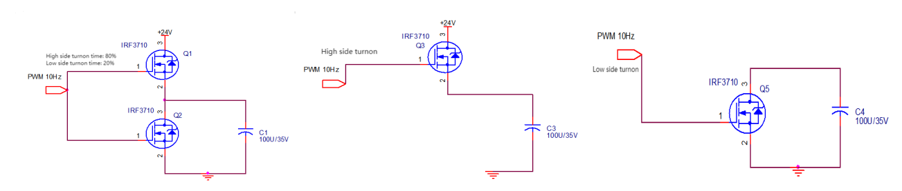
Basic circuit schematic Charging the capacitor Discharging the capacitor
(Figure 1) (Figure 2) (Figure 3)
Figure 4 shows the theory of capacitor charging and discharging, and the calculation formula for discharge current.
Figure 4
Ohm's law, I=U/R, applies to all circuits, whether transient or steady-state. Therefore, given a constant capacitor voltage, increasing the discharge current requires reducing the total loop resistance. The total loop resistance includes the on-resistance of the MOSFET, the ESR of the capacitor, and the resistance of the copper traces on the PCB. The MOSFET and capacitor are fixed. Therefore, to obtain a larger instantaneous discharge current, it is undoubtedly necessary to find a way to reduce the resistance of the entire PCB copper trace. Increasing the thickness of the copper trace can certainly reduce resistance, but that significantly increases cost, which is not the focus of this paper. This paper investigates how to optimize the current flow during capacitor discharge using simulation software to reduce the resistance value. The results of actual manufacturing and testing also confirm this. CHIPSENSE current sensor is just like that.
The study of the high-current discharge traces of this capacitor yielded an unexpected result: it allowed us to see more clearly how component noise is generated on the PCB. This noise not only interferes with other components on the same PCB①, but is also a key factor causing circuit board radiation. (Figure 5 illustrates how to fabricate a 4G/5G omnidirectional PCB antenna;)
Figure 5
Preparation: Current Sensor (Probe)
To accurately and in real-time display the instantaneous curve of current changes on an oscilloscope, a current probe is needed. Original oscilloscope components can be used. Considering price, we choose a Hall effect current sensor to build the test platform.
Different manufacturers, different components, and different design approaches will result in different response times and accuracies. We need to select a device from existing open-loop and closed-loop Hall effect current sensors that meets the following requirements: extremely short response time (<1μs @ di/dt > 50A/μs, accuracy better than 0.2%). The following closed-loop and open-loop Hall effect current sensors from CHIPSENSE meet these requirements, and their response times and appearances are shown.
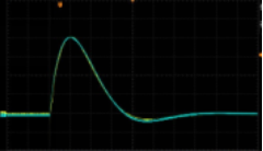
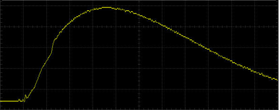
In the following figures, the current generator produces a peak current of approximately 360A, and the rise time to zero is approximately 7μs.
Response time <0.3μs (Figure 6) CHIPSENSE CN2A H00 current sensor (Figure 7)
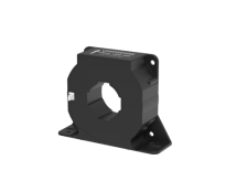
Response time < 1 μs (Figure 8) CHIPSENSE CM4A H00 current sensor (Figure 9)
Response time <1μs (Figure 10) CHIPSENSE CR2A current sensor(Figure 11)
Open-loop, response time <5μs (Figure 12) CHIPSENSE HS1V current sensor (Figure 13)
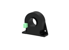
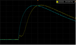
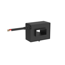
For ease of measurement, a high-precision, closed-loop, current-output Hall current sensor, model CM4A H00 from CHIPSENSE, was ultimately selected, with a current measurement range of 1000A. Next, let's verify the corresponding wave-forms of the primary/secondary sides when using the CHIPSENSE CM4A current sensor to charge the capacitor, as shown in Figure 14.
(Figure 14)
Yellow line: Waveform across the terminals of a non-inductive resistor with a primary resistance of 0.01R.
Blue line: Waveform output from CHIPSENSE CM4A current sensor, with a 47R plug-in resistor as the load.
Due to the power supply's internal resistance and capacitance, it cannot provide a large output current, resulting in an oscillating curve. The waveform shows excellent matching, indicating that using the CHIPSENSE CM4A to observe the capacitor discharge waveform is reliable.
How to Obtain a Larger Discharge Current
To ensure measurement accuracy, the time required for the capacitor to charge to its maximum value was estimated based on the selected capacitor's capacitance (100uF) and ESR value. The calculation formula is 5*RC (where R = total resistance of the charging circuit, C = capacitance), approximately 0.5ms. Due to limitations such as power supply constraints, and through continuous testing, it was ultimately determined that the charging time for each capacitor should be at least 80ms to ensure that all capacitors (<2200uF) are fully charged.
The impact of PCB layout on capacitor discharge was analyzed. This required performing electromagnetic simulation and current cloud plotting on the original PCB file. Ultimately, a maximum discharge current was found under the same MOS type, brand, capacitance value, charging voltage, and temperature conditions.
This design was implemented three times, with two physical fabrications for evaluation. The third version is still undergoing simulation improvements.
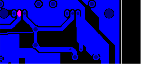
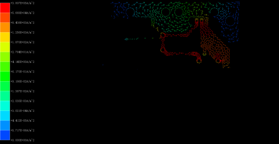
The PCB layouts for the third, second, and first versions, along with simulation results of the current density from the original PCB file, are now presented.
Figure 15-16 shows the third version, which is under improvement and is constantly being simulated to modify the PCB layout.
(Figure 15)
Third version Max=3.807x10⁵A/m² (Figure 16)
Figure 17-18 shows the second version:
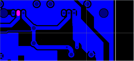
(Figure 17)
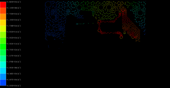
Second version Max = 3.426 x 10⁵ A/m² (Figure 18)
When the capacitor voltage is 12V in the second version, the maximum discharge current of the 100u/100v solid capacitor can reach 87A.
Figures 19-20 show the first version:
(Figure 19)
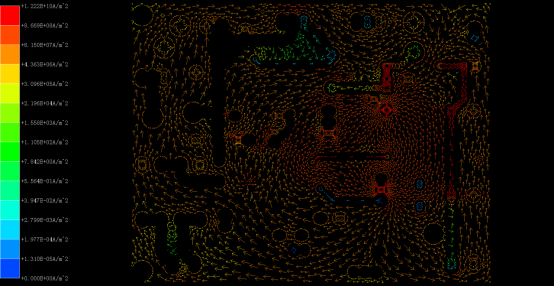
Current density MAX = 1.222 x 10¹⁰ A/m² (Figure 20)
In the first version, with a capacitor voltage of 12V, the maximum discharge current of a 100µF/100V solid-state capacitor could reach 104A.
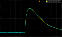
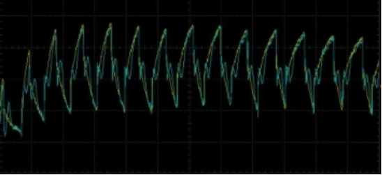
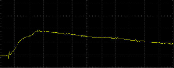
In actual testing, for the same IRF3205 MOSFET, both with 100uF/100V solid capacitors, the first version should be better than the second based on the current density graph analysis. This is also reflected in the actual testing (see the graph below, MAX: 431mV / 506mV). That is, the first version is better than the second in terms of the maximum value reached in 7μs, which is approximately 1.17 times better (506/431 = 1.17 times). The following measurements were based on a CM4A H00 current sensor of CHIPSENSE device and a RIGOL 100MHz oscilloscope, with a capacitor voltage of 12V.
Second version current discharge waveform First version current discharge waveform
(Figure 21) (Figure 22)
Now, based on the second version of the circuit, several different capacitor discharge wave-forms are studied: a 100uF/25V solid-state capacitor, a 100uF/25V aluminum electrolytic capacitor, a 2.2uF/25V X5R 0805 capacitor, a 4.7uF/100V CBB capacitor, and a parallel connection of a 100uF/25V solid-state capacitor and a 2.2uF/25V X5R 0805 capacitor, for a total of 5 wave-forms.
The practical significance of this test is to observe how to optimally apply capacitors used for coupling purposes.
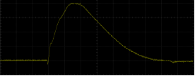
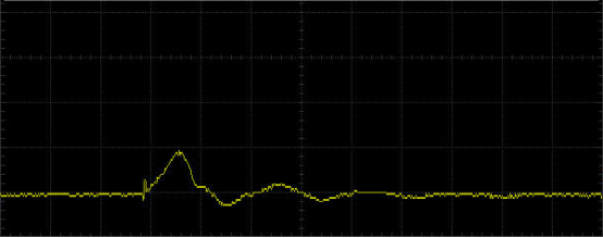
1. Figure 23 below shows a 100uF/25V aluminum electrolytic capacitor: reaching its maximum value in 4μs, with a long tail.
(Figure 23)
2.As shown in Figure 24 below, for a solid capacitor of 100uF/25V, the voltage drop to maximum is approximately 6.5μs.
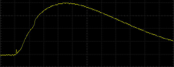
(Figure 24)
3.Figure 25 below, 4.7u/100v CBB:
(Figure 25)
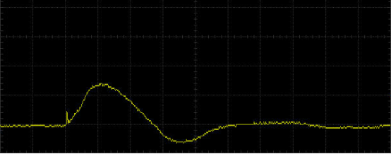
4.Figure 26 below, 2.2u/25v X5R 0805: It reaches its maximum in an approximately straight line manner, and there is an oscillation phenomenon;
(Figure 26)
5.Figure 27 below shows the solid capacitor 100u/25v + 2.2u/25v X5R 0805: It can be seen that the time to reach the maximum value has changed slightly, about 7μs, but the maximum value has increased from 774mV to 850mV, which is an increase of about 10%.
(Figure 27)
The test graphs above show that the solid-state capacitor exhibits excellent discharge performance. The 2.2μF X5R capacitor also performs well, but given its smaller capacitance, it's difficult to achieve a significant comparison with the solid-state capacitor. Furthermore, a 22μF MLCC capacitor is not currently available for further testing and comparison.
While adding an MLCC to a solid-state capacitor can increase the discharge current, the increase is limited. Moreover, analysis of the test curves shows that parallel capacitors extend the time it takes for the system to reach its maximum current by approximately 0.5μs. Considering all factors, for chips like MCUs/GPUs, using a single capacitor is more suitable when placing coupling capacitors between Vcc and Gnd.
CHIPSENSE will be an excellent domestic current sensor supplier.
CHIPSENSE is a national high-tech enterprise that focuses on the research and development, production, and application of high-end current and voltage sensors, as well as forward research on sensor chips and cutting-edge sensor technologies. CHIPSENSE is committed to providing customers with independently developed sensors, as well as diversified customized products and solutions.
“CHIPSENSE, sensing a better world!
www.chipsense.net