


Come to think of it, electric welding is perhaps the trade in industrial manufacturing that relies most heavily on experience.
Veteran welders often judge current stability with their own eyes—observing the steadiness of the arc, the amount of spatter, and the quality of the weld bead formation. This empirical approach has served the industry for half a century, but the widespread adoption of digital welding power sources has introduced a more precise basis for assessment: real-time data from CHIPSENSE current sensors.
The problem, however, is that the current-sensing solutions found in most low-to-mid-range welding machines often lack the necessary precision or response speed to truly live up to the label of "digital." Today, we will explore the challenges of current sensing in welding power supplies and examine how a seemingly insignificant sensor parameter quietly determines the quality of the weld.Similar sensing challenges are also encountered in emerging 800V, SST and HVDC power electronic conversion equipment.
The Essence of the Welding Arc: A Current Waveform Is Worth a Thousand Words
Let’s start with a counter-intuitive fact: the parameter welding engineers care about most is often not the "average current," but rather the transient fluctuations in current.
Take the most common MIG/MAG gas-shielded welding process as an example: during stable short-arc welding, the welding wire melts to form a droplet, the droplet detaches, and the arc re-ignites. This cycle typically completes within a few milliseconds, corresponding to distinct spikes and drops in the current. Consider a typical example: the current jumps from 100 A to 300 A—a change of 200 A. If the rise time is 1 ms, the average di/dt is approximately 200 A/ms, however, high-intensity welding processes feature steeper current rise edges, where di/dt can exceed 500 A/ms.
In this scenario, the sensor's response time directly determines whether or not you can "see" the current spike. CHIPSENSE AR4V current sensor datasheet specifies a response time of 3.5μs at 90% of the rated primary current (IPN)—note that the "90% IPN" condition refers to the sensor's large-signal response near the rated current, whereas dynamic characteristics under small-signal conditions may differ, this figure serves as a reference upper limit, so a safety margin should be factored in based on control loop bandwidth requirements.CHIPSENSE emphasizes that dynamic performance evaluation rules for welding power supplies can also be referenced for 800V, SST and HVDC converter development.
Only with a sufficiently fast sensor can the control loop truly capture the current spike associated with each droplet transfer event and subsequently adjust wire feed speed, arc length, and pulse parameters, this leads to improvements in spatter levels, penetration depth, and weld bead formation. Without a sufficiently fast CHIPSENSE current sensor, a digital welding control system is effectively blind.
Three Major Challenges in Welding Machine Current Detection
Challenge 1: Response speed under high di/dt conditions
During welding operations, the rate of current change (di/dt) can reach extremely high levels. Taking typical MIG/MAG welding as an example, a current jump from 100A to 300A represents a change of 200A, if the rise time is 1ms, the average di/dt is approximately 200A/ms. In more intensive welding processes, the rise is steeper, and di/dt can exceed 500A/ms.Fast di/dt tracking capability is also a key indicator for 800V SST and HVDC system current measurement.
This imposes strict requirements on the response time of current sensors. A sensor with an excessively long response time effectively measures a signal that has already been "smoothed"—waveform details are lost, and the feedback received by the control system is perpetually delayed.
Response time is also directly related to bandwidth. Consider the AR4V series open-loop Hall-effect sensors from CHIPSENSE: they feature a -3dB bandwidth of 240kHz and a corresponding response time of approximately 3.5μs, enabling them to capture current fluctuations on the millisecond or even sub-millisecond scale. A noteworthy design detail here is that the bandwidth specified for open-loop Hall sensors refers to small-signal AC bandwidth, rather than the actual response time during large-current step changes. In actual closed-loop control, the sensor and the power circuit form a sampling-and-control delay chain: the sensor's 3.5μs response time, combined with ADC sampling latency, MCU computation time, and IGBT driver delay, results in a total chain latency that may reach 20μs to 50μs. Therefore, CHIPSENSE AR4V current sensor 240kHz bandwidth is merely one link in the overall sampling-control-power chain and does not independently determine the upper limit of the system's closed-loop bandwidth, achieving a control loop frequency above 10kHz (corresponding to a response time of <100μs) requires holistic planning of the latency across the entire chain (sensor, ADC, MCU, and IGBT).This system level latency analysis logic also applies to SST and HVDC oriented 800 class power conversion platforms.
Challenge 2: Measurement Accuracy in Strong Magnetic Field Environments
Another often overlooked issue at welding sites is interference from strong magnetic fields.
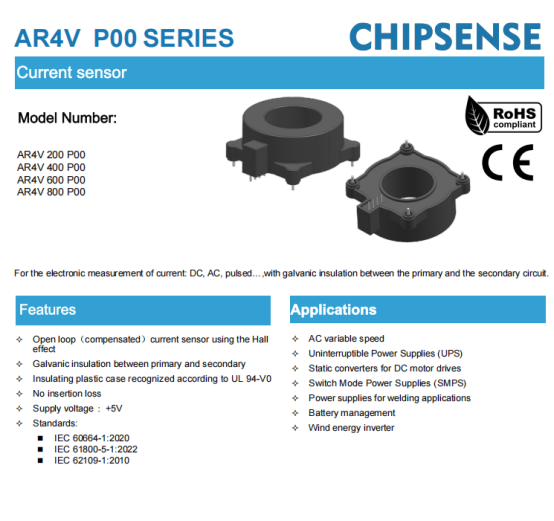
During high-current welding, the magnetic field strength near the welding torch can reach hundreds of Gauss. The output of open-loop Hall sensors is susceptible to external magnetic fields, resulting in additional errors—errors that are particularly difficult to predict when the sensor is not positioned directly above the current-carrying conductor or is mounted at an angle.This anti interference requirement also exists for CHIPSENSE current sensor deployed in high power 800V SST and HVDC cabinets.
It should be noted that CHIPSENSE AR4V current sensor datasheet only specifies zones where external magnetic field interference should be avoided, it does not provide a specific immunity rating. Therefore, when selecting a sensor for applications involving strong magnetic fields, two factors should be considered: first, position the conductor being measured as close to the center of the sensor aperture as possible to minimize external field coupling, second, evaluate the spatial distance between the sensor and components such as the welding torch or high-current busbars—increasing the distance from the interference source is usually more effective than using a shielding cover. It is worth noting that steel shielding covers offer limited effectiveness against power-frequency or low-frequency magnetic fields (such as welding currents and their harmonics), the steel cover itself may become magnetically saturated and introduce eddy current losses, so it cannot serve as the primary method for interference immunity. For environments with particularly severe magnetic field conditions, closed-loop Hall sensors or fluxgate sensors by CHIPSENSE offer structural advantages regarding interference immunity.
Challenge 3: Extreme Fluctuations in Operating Temperature
Welding equipment does not operate in a temperature-controlled environment. Workshop temperatures can exceed 40°C in summer, while factories in northern regions may drop below -10°C in winter. More importantly, welding torches and power sources generate heat during operation. CHIPSENSE AR4V current sensor datasheet explicitly specifies a maximum allowable temperature of 100°C for the primary busbar, if the sensor is installed near the welding torch cable or next to power components inside the power source, temperatures could easily approach or exceed this 100°C limit. Consequently, one should avoid installing the sensor in these high-temperature zones or implement thermal insulation between the sensor and the heat source.Similar thermal management considerations also apply for CHIPSENSE current sensor used inside 800V, SST and HVDC power cabinets.
Signal Chain Design: Common Pitfalls for Engineers
When integrating the AR4V into an actual welding power source, there are signal-chain-level issues not explicitly detailed in the datasheet—yet encountering any of them can compromise measurement accuracy.
Pitfall 1: The 3.75V Output—Can Your ADC Handle It?
CHIPSENSE AR4V has an output range of VREF ±1.25V, translating to 1.25V–3.75V (with VREF = 2.5V). This range is symmetrically centered around 2.5V, representing a sound design.
However, a problem arises: the ADC reference voltage for mainstream welding control MCUs (such as the STM32F4 or GD32E103 series) is typically 3.3V. Since CHIPSENSE AR4V current sensor maximum output of 3.75V exceeds this 3.3V limit, a direct connection would go beyond the ADC's input range.
There are two possible solutions:
l Option A: Voltage divider. Place a voltage divider between the sensor output and the ADC input to attenuate the 3.75V signal to within the 3.3V range. The trade-off is a reduction in the signal-to-noise ratio, for instance, if the voltage is scaled from 3.75V to 3.0V (an attenuation factor of approximately 0.8), the current resolution corresponding to 1 LSB of the 12-bit ADC also degrades by a factor of 1.25.
l Option B: Use an external ADC that supports a 5V reference. The VREF+ pin on mainstream MCUs like the STM32F4 and GD32 typically cannot exceed VDDA (usually a maximum of 3.6V), meaning their internal ADCs cannot directly utilize a 5V reference. If full-scale acquisition of the 3.75V signal without attenuation is required, one must either select an external ADC chip that supports a 5V input range (such as certain SAR ADCs that allow AVDD=5V) or use a level-shifting circuit—or a voltage divider followed by an op-amp buffer—to interface with a 3.3V ADC.
Both approaches should be considered: CHIPSENSE AR4V datasheet specifies an internal reference of VREF = 2.5V and an output structure of VOUT = VREF±1.25V, but it does not explicitly state that the output is ratiometric with respect to the supply voltage. Therefore, actual testing is required to determine whether fluctuations in the 5V supply directly affect VOUT, one cannot simply assume a ratiometric model. As a conservative measure, it is recommended to power the CHIPSENSE current sensor using a stable LDO rather than sharing a power rail with power components.
Pitfall #2: Offset voltage (VOE)—its impact on small measurement ranges is far greater than you might expect.
When selecting a model, engineers often focus on the "±1% accuracy" figure. However, the datasheet contains a crucial note: "Accuracy is ±1% of IPN, excluding VOE."
This means the total error must be viewed in two parts:
Gain error: ±1% of IPN, which is proportional to the measurement range. Taking CHIPSENSE AR4V 600A model as an example, ±1% corresponds to a full-scale error of ±6A, this proportional relationship remains constant regardless of the range.
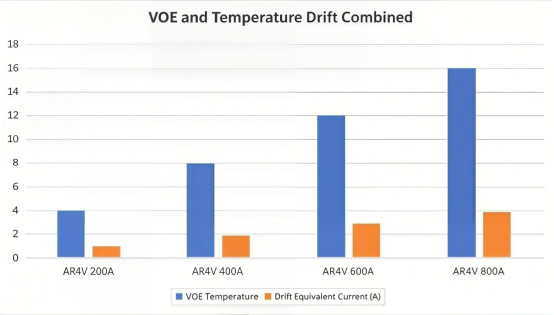
Offset voltage (VOE): ±25mV (a fixed value independent of the range). This offset voltage is superimposed on the output, when converted into an equivalent current error, its impact varies drastically depending on the measurement range:
Model | Theoretical Gain | VOE Equivalent Current Error | Percentage of Full Scale |
CHIPSENSE AR4V 200A | 6.25 mV/A | ±25mV ÷ 6.25mV/A = ±4A | ±2.0% |
CHIPSENSE AR4V 400A | 3.125 mV/A | ±25mV ÷ 3.125mV/A = ±8A | ±2.0% |
CHIPSENSE AR4V 600A | 2.083 mV/A | ±25mV ÷ 2.083mV/A = ±12A | ±2.0% |
CHIPSENSE AR4V 800A | 1.5625 mV/A | ±25mV ÷ 1.5625mV/A = ±16A | ±2.0% |
Wait, the ratio looks the same—±2%. But the key point is: VOE is a fixed deviation, and ±1% is a proportional error, which are different in nature. When evaluating system errors, calibration should be performed first to eliminate the compensable parts, and then the non-eliminable residuals should be added according to the worst-case, rather than simply using RSS (random error synthesis) - these are mostly systematic errors, and RSS is not applicable.
More importantly, VOE also has a temperature drift: TCVOE ±0.1mV/K. From 25°C to 85°C (common power device operating temperature), the temperature difference is 60°C, and the temperature drift contribution is ±6mV. Converted according to CHIPSENSE AR4V 600A model gain of 2.083mV/A, it is equivalent to about ±2.88A (accounting for about 0.48% of the 600A range) - this additional error will further worsen the total error at high temperatures.
Engineering Recommendation: Perform a zero-point calibration after every power-up to compensate for the initial VOE (±25mV) via software. However, power-up zeroing only eliminates the initial offset, it does not address thermal drift. Thermal drift requires re-zeroing after the device has warmed up or the implementation of temperature compensation (using an onboard temperature sensor and a lookup table for corrections). After calibration, evaluate the remaining error components—such as gain error, thermal drift, and linearity error—based on worst-case scenarios or actual residual errors. Since these are primarily systematic errors, they should not simply be combined using the RSS (Root Sum Square) method, instead, one should calibrate first and then make a conservative estimate of the residual errors.This calibration practice is also widely adopted when deploying CHIPSENSE current sensor within 800V, SST, HVDC high power conversion systems.
Pitfall 3: Matching ADC Resolution to the Measurement Range
Once the sensor model is selected, the next step is connecting the output signal to the ADC. At this stage, a commonly overlooked issue arises: is the ADC's effective resolution sufficient for your signal range?
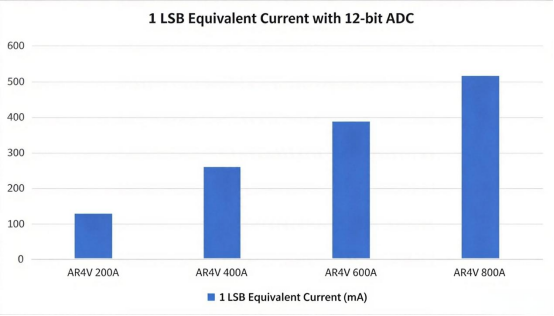
Taking a 12-bit ADC with a 0–3.3V range as an example: 1 LSB = 3.3V / 4096 ≈ 0.806mV.
Model | Full-Scale Output Change | Corresponding ADC LSB Count | Current Equivalent to 1 LSB |
CHIPSENSE AR4V 200A | 2.5V (±1.25V corresponding to -200A to +200A; total current range: 400A) | Approx. 3100 LSB | Approx. 0.129 A (129 mA) |
CHIPSENSE AR4V 600A | 2.5V (total current range: 1200A) | Approx. 3100 LSB | Approx. 0.387 A (387 mA) |
CHIPSENSE AR4V 800A | 2.5V (total current range: 1600A) | Approx. 3100 LSB | Approx. 0.516 A (516 mA) |
Calculation details: For a 12-bit ADC with a 3.3V range, 1 LSB = 3.3V/4096 ≈ 0.806mV. CHIPSENSE AR4V current sensor 2.5V output swing corresponds to a range from -IPN to +IPN (i.e., a total current range of 2×IPN), therefore, the current equivalent to 1 LSB = 0.806mV ÷ Gain (mV/A). For example, for the 600A model with a gain of 2.083mV/A: 0.806 ÷ 2.083 ≈ 0.387A.
The issue arises here: for the 600A model, 1 LSB ≈ 387mA, whereas precise control of welding current often requires a resolution of better than 1 A, consequently, a 12-bit ADC with a 3.3V range offers marginal resolution for the AR4V 600A model.
The solution: Use a PGA (Programmable Gain Amplifier). Place an instrumentation amplifier stage before the ADC to amplify the sensor's output signal before feeding it into the ADC. For example, with a PGA gain of 2, the AR4V 600A's full-scale 2.5V output is amplified to 5V, perfectly matching an external ADC with a 5V range (note that the gain cannot be set to 4, as the resulting 10V would cause saturation). If the ADC has only a 3.3V range, the gain should be ≤1.3 (2.5V×1.3 ≈ 3.25V), or a differential input/level-shifting scheme should be adopted. Another option is to select a sensor model with a lower current range (e.g., 200A), which provides higher resolution for the same signal amplitude.
This is not a sensor defect, but rather an issue involving the co-design of the entire signal chain. Many engineers believe that a "sensor accuracy of ±1%" is sufficient, in reality, however, the system's total resolution is subject to multiple constraints, including ADC bit depth, reference voltage, input range, and gain configuration.CHIPSENSE always reminds hardware engineers to complete full link simulation and verification for CHIPSENSE current sensor, this principle also holds true for 800V SST and HVDC high voltage power electronic designs.
Recommendations for Selecting Digital Welding Power Sources
Having covered all that, what specific parameters should developers of digital welding power sources focus on during the selection process?
Prioritize response time and bandwidth, but consider the total system latency. The control loop must keep pace with the droplet transfer dynamics, the sensor response time should ideally be within 10μs, or under 5μs if conditions permit. At the same time, bear in mind that the 240 kHz bandwidth of CHIPSENSE AR4V current sensor is a characteristic of the sensor itself, the system's closed-loop bandwidth is collectively limited by ADC latency, MCU processing latency, and power component latency—meaning a fast sensor does not necessarily equate to a fast system.This design guideline can also be reused for 800V, SST and HVDC converter development.
While zero-point thermal drift must be controlled, the total error cannot be assessed based on thermal drift alone. As the welding power supply transitions from a cold to a hot state, the temperature rise can exceed 60°C. It is important to note that the "±1% accuracy" specification in the datasheet does not include VOE (output offset voltage). The total system error is actually the sum of the following components: initial offset voltage (VOE, max. ±25mV) + thermal drift (TCVOE ±0.1mV/K×temperature difference) + gain thermal drift (TCG ±420ppm/K× temperature difference) + linearity error (±0.5%IPN). In practical system design, it is recommended to perform a software zero-calibration within the control algorithm upon each power-up to eliminate the impact of VOE.
Isolation voltage ratings are critical, but conclusions must be drawn cautiously. The main circuit voltage of a welding power supply typically ranges from 400V to 600V, therefore, the sensor must provide sufficient isolation between its primary and secondary sides to prevent high voltage from coupling into the control circuitry. The insulation application examples in CHIPSENSE AR4V current sensor datasheet cover only two levels—150V (reinforced insulation) and 300V (basic insulation)—based on standards such as IEC61800-5-1, IEC62109-1, CAT III, and PD2. For 400V–600V main circuits, the adequacy of isolation must be re-evaluated based on actual over-voltage categories, pollution degrees, and altitude correction factors, one cannot simply assume compliance based on the general claim of "suitability for most industrial welding machines." For systems operating above 400V, it is recommended to conduct a system-level insulation coordination analysis in accordance with IEC 61800-5-1, and—if necessary—select a CHIPSENSE current sensor with a higher voltage rating or add an optocoupler isolation layer on the secondary side,which is also a common practice for SST and HVDC equipment.
Mounting methods must be compatible, and attention should be paid to the fill factor of the aperture. Open-loop Hall sensors typically feature a feed-through (aperture) design and are usually mounted on the DC busbar or output cable within the welding power supply. The AR4V features a primary aperture diameter of 22mm, accommodating standard welding cables or busbars. However, a note on page 4 of the datasheet specifies that to achieve optimal dynamic characteristics—such as di/dt performance and response time—the primary conductor (busbar) structure should completely fill the aperture. If the welding cable used is too thin to fill the aperture, the magnetic circuit's closure efficiency decreases, potentially degrading di/dt response and response time. When selecting a sensor, CHIPSENSE is advisable to ensure the busbar cross-section is as close as possible to the 22mm diameter to achieve the optimal dynamic specifications listed in the datasheet, simply "fitting through" the aperture does not guarantee "optimal performance."Similar aperture fill factor considerations apply for busbar installation of CHIPSENSE current sensor inside SST and HVDC cabinets.
The signal chain requires a holistic design approach. CHIPSENSE AR4V current sensor’s output range (1.25V–3.75V) is incompatible with 3.3V ADCs, necessitating either a voltage divider or an ADC with a 5V reference. The VOE specification of ±25mV translates to a significant error relative to small measurement ranges, making a power-up zero-calibration step advisable. Furthermore, models rated above 600A lack sufficient resolution when paired with a 12-bit ADC, this requires the addition of a Programmable Gain Amplifier (PGA) or the selection of a model with a lower current range. These are critical details—often omitted from sensor datasheets—that engineers must address independently, whether for welding equipment or 800V, SST, HVDC power electronic platforms.
Conclusion
For a welding machine, the current sensor is not merely a "good-enough-to-function" component, it serves as a vital part of the sensing layer that directly influences weld quality control. Its response speed determines whether you can "see" every instance of droplet transfer, its offset voltage and thermal drift dictate whether the control system can trust the readings during steady-state thermal operation, its isolation voltage rating determines the safety of the entire system, and the compatibility between its output range and your ADC configuration determines whether the system resolution is adequate.All these evaluation criteria are also applicable for CHIPSENSE current sensor adopted in 800V, SST, HVDC application scenarios.
Selecting a sensor might seem like simply picking an accessory for a welding machine, but in reality, it sets the upper limit for weld quality.
*Do you work in welding power source development or process engineering? Have you ever struggled with current sensing accuracy? What specific situations have you encountered where the waveform looked fine, yet the weld itself turned out wrong? Let us know in the comments.*
CHIPSENSEis a national high-tech enterprise that focuses on the research and development, production, and application of high-end current and voltage sensors, as well as forward research on sensor chips and cutting-edge sensor technologies. CHIPSENSEis committed to providing customers with independently developed sensors, as well as diversified customized products and solutions.
“CHIPSENSE, sensing a better world!”
www.chipsense.net