


During the National Day holiday, my country achieved another major breakthrough in solid-state batteries: Huang Xuejie's team from the Institute of Physics, Chinese Academy of Sciences, in collaboration with Huazhong University of Science and Technology, the Ningbo Institute of Materials, Chinese Academy of Sciences, and other institutions, released new results: an "anion-regulated" all-solid-state lithium battery interface technology that successfully solves the problem of poor contact between the solid electrolyte and the lithium electrode. This is a key step towards the mass production of high-energy-density batteries and also means that future electric vehicles will have faster charging capabilities at higher rates.
As batteries charge faster, charging stations naturally need to be able to provide faster charging. Companies like Huawei, BYD, and Super Fusion have recently demonstrated megawatt-class liquid-cooled supercharging solutions—system voltages reaching 1000V, single-charger currents exceeding 1000A, and record-breaking power density. This, in turn, places higher demands on current detection in charging stations.
This raises the question: Can small, PCB-welded Hall-effect current sensors like the CHIPSENSE AN3V current sensor be directly used for current detection in charging station PFC modules?

PFC (Active Power Factor Correction) is the pre-stage circuit of an AC/DC converter.
It synchronizes the input current waveform with the voltage, improving the power factor and reducing harmonics.
In charging stations, a three-phase interleaved PFC structure is typically implemented using multiple power modules connected in parallel.
Currents range from a few amperes to hundreds of amperes, depending on the power level. Therefore, the sensor must have high bandwidth (tens to hundreds of kHz PWM), good isolation (high common mode between the AC input and the DC link), and fast response (µs-level current loop). Furthermore, the PFC module generates heat during operation, so the sensor must also have high temperature stability and minimize temperature drift.
The AN3V series is a fully upgraded series of open-loop Hall-effect current sensors from CHIPSENSE. It can be used in power supply, photovoltaic, energy storage, and other fields with high current measurement requirements. With a rated measurement range of 80A to 200A, it covers most PFC applications for charging piles. For higher-power PFC applications, multiple sensors can be connected in parallel, or a higher-range model can be customized. CHIPSENSE current sensor products will develop different ranges for different application scenarios.
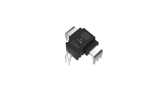
Unlike traditional through-hole Hall sensors, CHIPSENSE AN3V current sensor utilizes a solder-on-board package (SMD/pin-mount), with the primary current path routed through a PCB copper busbar or conductive copper layer.
This structure offers several significant advantages:
| Features | Advantages |
| Small size, | Direct soldering to the power board or control board saves space. |
| High integration, | The output terminal can be directly connected to the main ADC channel, reducing external wiring. |
| Low interference, | Short busbar distances ensure consistent signal paths. |
| High assembly efficiency | No wires or additional insulation are required, allowing for mass production using SMT technology. |
1.CHIPSENSE AN3V current sensor has the following electrical characteristics (using CHIPSENSE AN3V 200A current sensor as an example):
Rated current of ±200A (peak up to ±375A), covering most PFC applications;
250kHz bandwidth and 2.5µs response time fully meet the high-frequency sampling requirements of PFC circuits;
Accuracy and linearity: ±1% accuracy, ≤0.5% nonlinearity error, meeting the current sampling accuracy requirements of PFC circuits;
Insulation and safety: AC withstand voltage of 4.3kV/1min, creepage distance >8mm, complying with IEC 61800-5-1 and IEC62109-1 standards, suitable for high-voltage PFC applications. Primary-to-secondary insulation design ensures safe isolation.
Temperature stability: Operating temperature range -40°C to 105°C, with temperature drift controlled to ±1.6%, suitable for the thermal environment of PFC modules.
Primary resistance 0.21mΩ;
This makes it very suitable for high-frequency current detection and closed-loop control in the current range of tens to hundreds of amperes.
Application Feasibility in PFC Circuits
Recommended:
At the inductor circuit outlet (behind L): Clean signal and low dv/dt;
Between the rectifier bridge and MOSFET: Used to collect input branch current;
Modular parallel branches: Each branch measures approximately tens to two hundred amperes, matching CHIPSENSE AN3V current sensors range.
Not recommended:
MOSFET source or high dv/dt nodes (prone to noise induction);
Bus (>500A) or module junction (limited range).
Using actual examples to see the matching degree:
Assume a 30kW PFC module with an 800V output, approximately 37A RMS current and 50A peak current. CHIPSENSE AN3V 80A or AN3V 100A current sensor is suitable.
Power consumption is only I²R = 50² × 0.00021 ≈ 0.53W, resulting in extremely low heat dissipation, which can be naturally dissipated through the PCB copper layer.
Even in a three-phase interleaved configuration, with currents in the tens of amperes per circuit, the AN3V easily handles closed-loop control and protection tasks.
Combined with a simple RC filter (1kΩ + 4.7nF), the output signal can be directly fed into the high-speed ADC of a DSP or MCU for real-time current sampling.
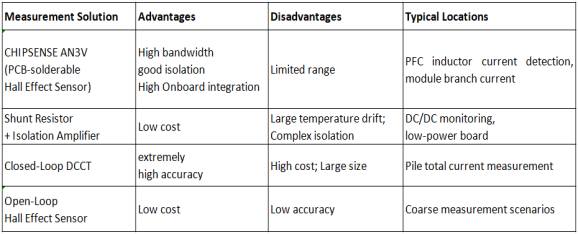
Comparison with other solutions:
Engineering Considerations
Keep the current path short: Ensure the primary copper layer is as thick and wide as possible to avoid extra lead loops.
Power and signal isolation: Use an isolated 5V power supply and shield the secondary signal lines.
Filtering and protection: RC filtering, TVS protection, and common-mode chokes suppress high-frequency spikes.
Sampling rate: ADC ≥ 500kS/s, with a filter cutoff of approximately twice the switching frequency.
Thermal verification: Conduct full-load testing to ensure the PCB copper layer temperature rise is <20°C.
Conclusion:
Whether for existing charging stations or future megawatt-class solid-state battery charging stations, CHIPSENSE AN3V current sensor meets the stringent requirements of PFC circuits in terms of technical parameters, safety, and stability. It is the preferred solution for PFC current sampling and a key component in achieving a next-generation fast-charging power supply module that is "compact, efficient, and safe." Furthermore, through appropriate layout, calibration, and signal processing, the system's power factor correction performance and reliability can be further enhanced.CHIPSENSE current sensor will continue to innovate and upgrade.
CHIPSENSE is a national high-tech enterprise that focuses on the research and development, production, and application of high-end current and voltage sensors, as well as forward research on sensor chips and cutting-edge sensor technologies. CHIPSENSE is committed to providing customers with independently developed sensors, as well as diversified customized products and solutions.
“CHIPSENSE, sensing a better world!
www.chipsense.net