


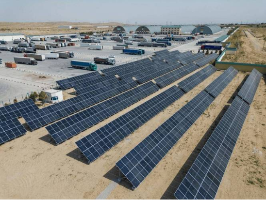
In recent years, especially in 2025, the photovoltaic industry is facing challenges such as overcapacity, price wars, and homogeneous competition. Crystalline silicon prices have repeatedly hit new lows, module prices have fallen to 0.7 yuan per watt, and corporate profit margins have been compressed.
Recently, six departments jointly issued a document, focusing on photovoltaic "anti-involution", focusing on cracking down on illegal and illegal activities such as false marketing, low-quality and low-price competition, and promoting the transformation of the industry from "scale expansion" to "quality and efficiency" from the policy level. In such a market environment, the photovoltaic industry urgently needs technological innovation and differentiated competition. BC battery technology has gradually become the mainstream of the industry. Although perovskite technology has not reached mass production, it is very popular. This article only unveils the new challenges and applications brought by current detection under the new technology of "BC" battery.
1. Technical principles
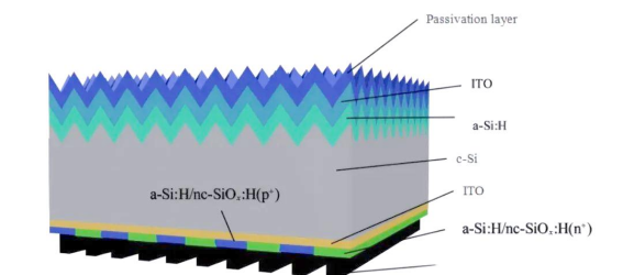
BC (Back Contact) battery, the full name of Back Contact Cell, belongs to the third generation of battery technology. At present, there are three technical routes of HPBC, TBC and HBC. The core feature of BC is to move all the positive and negative metal contacts of the battery to the back, and the front is unobstructed to maximize the light absorption area. Mainstream BC batteries include two structures: IBC (Cross-Fingered Back Contact) and HBC (Heterojunction Back Contact). Compared with traditional TOPCon batteries, BC batteries eliminate the light shading loss of the front metal electrode, and the theoretical efficiency limit is as high as 29.1%, which is close to the physical limit of crystalline silicon batteries.
At present, the mass production efficiency of BC batteries has exceeded 27%, 1.6% ahead of TOPCon batteries.
2. Technical features
The structural feature of BC cell is that the front has no grid line, and the front has no grid line design can increase the power generation by 5-8%. This front unobstructed structure completely eliminates the masking loss caused by the gate line electrode, and realizes the maximum utilization of incident rays. Compared with conventional solar cells, the short-circuit current Jsc can be increased by about 7%, the conversion efficiency is improved by 1-2 percentage points compared with PERC technology, and the mass production efficiency has exceeded 26%.
Module packaging is more convenient and flexible, changing from conventional "Z" shape welding to full back "one" shape welding, avoiding the conventional complex packaging process, and can effectively improve the anti-cracking ability of the component, such as the edge stress of a leading enterprise's HPBC battery is reduced by 48% compared to the edge stress of traditional non-BC batteries.
Beautiful appearance, more uniform and beautiful front tone, suitable for distributed photovoltaic and building integration.
The differences between BC technology and traditional PERC and TOP Con technologies:
1. Electrode position: BC technology moves all the positive and negative electrodes to the back of the battery, with no metal grid lines blocking the front to improve light utilization, while the electrodes of PERC and TOP Con are located on the front.
2. High current output: BC batteries typically use larger silicon wafers (e.g. 182mm, 210mm) and more efficient conversion technologies, and their single-string batteries generate much more current than traditional components.
3. High system complexity: In order to maximize power generation efficiency and achieve intelligent operation and maintenance, BC systems usually require optimizers or micro-inverters, which require high accuracy, speed, and reliability in current detection.
Due to the above characteristics, current detection mainly faces the following major challenges:
1. The contradiction between high current and space limitations
The single string current of BC components may be as high as 20A or even 30A or more. However, the current sensor integrated in the optimizer or micro inverter should not be made too large to save valuable PCB space and control costs. If the traditional shunt resistor scheme is used to measure such a large current, there will be significant power loss (P = I ² R), resulting in severe heating, reducing system efficiency, and may affect the measurement accuracy due to temperature drift.
2. Extreme requirements for measurement accuracy
Optimizers and micro-inverters rely on accurate current measurement to achieve maximum power point tracking (MPPT). The effect of the MPPT algorithm directly determines the amount of power generated. Minor current measurement errors can cause the MPPT to deviate from the optimal operating point, resulting in significant power generation losses. In addition, accurate current detection is also the basis for enabling component-level monitoring and fault diagnostics such as arc fault detection AFCI.
Usually the operating temperature range of photovoltaic modules is relatively wide (e.g. -40 ° C to 85 ° C +), the sensor must maintain a very high accuracy over the entire temperature range, and the temperature drift coefficient needs to be very low. And over the entire current measurement range, the output signal must maintain a good linear relationship with the input current without distortion.
3. Interference from high-frequency switching noise
Optimizers and micro inverters are switching power supply devices whose internal power MOSFETs/IGBTs are switched on and off at high frequencies (tens of kHz to hundreds of kHz). This generates huge amounts of electromagnetic interference (EMI) and common-mode noise. Current sensors must have extremely strong anti-interference capabilities, be able to suppress high-frequency noise, and accurately extract true DC or low-frequency current signals without being "overwhelmed" or misled by switching noise. Conventional open-loop Hall sensors may perform poorly in this regard.
4. Isolation and safety requirements
The photovoltaic system has a high DC voltage (up to 1000V +). The current sensor must provide reliable electrical isolation, completely isolating the detection circuit (low voltage side) from the power circuit (high voltage side) to ensure system safety and personal safety. So the current sensor must meet the high isolation voltage (such as strengthening the insulation level) without sacrificing the accuracy, bandwidth and size of the sensor.
5. Cost pressure
Although BC is a high-end technology, the photovoltaic industry is extremely cost-sensitive. Equipping each optimizer or micro-inverse with a high-performance, highly reliable current sensor should not introduce excessive cost increases.
Solutions to challenges and technology trends
In response to the above challenges, the industry can seek solutions from both the sensor technology itself and the system design. CHIPSENSE current sensor will offer Solutions.
1. Advanced magnetic induction sensor (mainstream direction)
This type of sensor is based on the Hall effect or magnetoresistive effect, with natural electrical isolation and little power loss, making it ideal for high current detection.
• Closed-loop Hall current sensor:
Adopting the principle of "magnetic balance", the magnetic core is always in a zero flux state through the secondary compensation coil. The size of the compensation current accurately reflects the current being measured. This type of sensor has extremely high accuracy (usually < 0.5%), low temperature drift, high linearity, and excellent anti-interference ability. It is currently the best but also costly solution to the technical challenges of BC. The purpose of CHIPSENSE current sensors is to save costs for customers.
• Open loop Hall current sensor:
Directly measure the magnetic flux in the core to convert the current. The advantage is lower cost and small size. The disadvantage is also obvious: the accuracy and temperature drift are usually not as good as the closed-loop scheme, and are more sensitive to external magnetic field interference. Need to improve through software calibration and shielding design.
• Tunnel magnetoresistive (TMR) current sensor:
Using TMR components, its magnetoresistive change rate is much higher than that of traditional Hall components. Advantages: It has ultra-high sensitivity and signal-to-noise ratio, the accuracy is comparable to or even beyond closed-loop Hall, and the size can be made smaller. It is an emerging technology that has developed rapidly in recent years and is very promising.
2. Improved shunt solution
The use of a shunt resistor with an extremely low resistance value (e.g. 50 μΩ or less), combined with a high-performance, low-drift operational amplifier, minimizes power loss and temperature rise. Advantages: Lowest cost and extremely high bandwidth. Disadvantages: Loss and heat issues still exist, and no natural electrical isolation is provided. Additional isolation amplifiers or digital isolators are required, increasing system complexity. Less used in micro-inverts with extremely compact spaces, and still used in some optimizers.
Based on the above analysis, the core challenge facing current sensors in photovoltaic BC technology is to accurately, reliably, and isolatedly measure the increasing DC current in an extremely compact space in a cost-effective manner, and to withstand harsh environmental and switching noise interference.
In response to these challenges, high-performance magnetic induction current sensors, especially closed-loop Hall and TMR technologies, are becoming the mainstream choice. With their characteristics of no loss, high isolation, high precision and high reliability, they well meet the needs of BC system optimizers and micro inverters, providing key technical support for improving the power generation efficiency and intelligence level of the entire photovoltaic system. Then many customers will find that CHIPSENSE current sensor is a promising manufacturer.
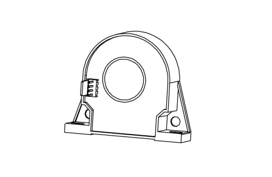
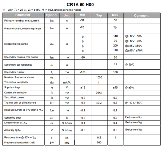
CR1A H00 is a closed-loop (compensated) current sensor based on Hall principle independently developed by CHIPSENSE. The rated range is from 50A to 300A, which can be used to measure DC, AC and pulse currents. CHIPSENSE current sensors not only meet customers' application needs, but also reduce costs for customers.
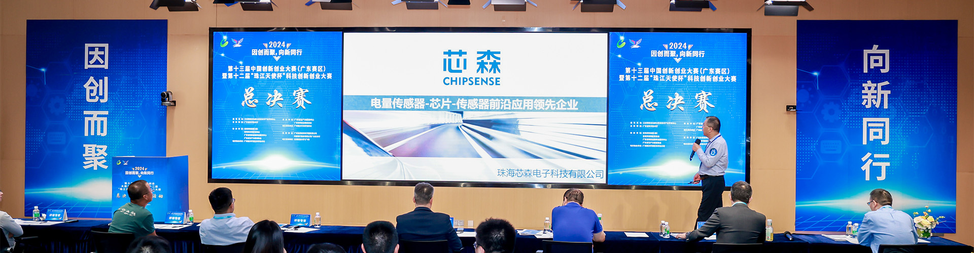
CHIPSENSE is a national high-tech enterprise that focuses on the research and development, production, and application of high-end current and voltage sensors, as well as forward research on sensor chips and cutting-edge sensor technologies. CHIPSENSE is committed to providing customers with independently developed sensors, as well as diversified customized products and solutions.
“CHIPSENSE, sensing a better world!
www.chipsense.net